


Best viewed using:
Internet Explorer
or
Mozilla Firefox


Wiring our Micro LEDs
If you've wired up some of our 2x3 LEDs, you've gained the general techniques required to wire up our Micro (or Nano) LEDs. The solder pads are much smaller (as are the LEDs), but with good magnification (here we go again...), all of the same steps apply. If you need to review wiring procedures for our 2x3's, direct links are here and here.
CAUTION!
Our RED Micro, Nano and Subminiature LEDs are wired differently than all of our other LEDs. The polarity mark on the LED is for the ANODE (+) connection, not the CATHODE (-) connection.
Let's wire up a Micro LED
Following is a graphic step-by-step wiring of a Micro LED using our NT301 Holding Tool. The wire routing method shown, we refer to as "back wiring" (for lack of a better term). The wires are routed directly away from the back of the LED. This is a useful wiring method, for example, if we were going to build a streetlight or building light and want the LED facing down from the inside of a lampshade, or to face down from the ceiling of a building interior.
-
Our LEDs are packaged in a black conductive plastic carrier strip. This strip contains pockets, or cavities that contain the individual LEDs and are held in place by a clear plastic cover-strip that can be pealed back to remove the LEDs. The reason that the carrier strip is conductive is that the LEDs are static electrically sensitive devices. Therefore, before removal or handling of the LEDs, precautions to prevent static discharge should be taken (good grounding, anti-static mat or wrist strap, etc). Please review the packaging and handling procedure here.
-
Once an LED has been removed from its protective carrier and placed in some temporary receptacle, orient the LED so it is "face up" (solder pads and circuit board side facing down) in the receptacle. we are now ready to carefully grasp the part with tweezers and position it for wiring. Since we will be using our Holding Tool, we will transfer the LED from its temporary receptacle to a riser block as shown in Figure 1 below.
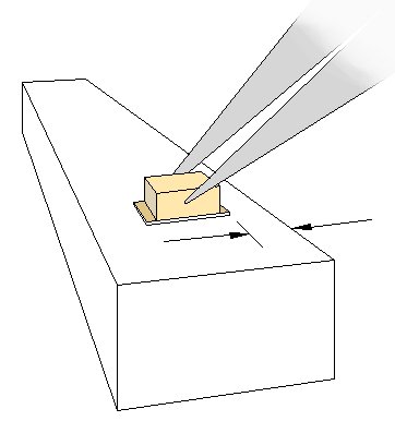
Figure 1
-
This riser block is used to space the LED above the workbench so our Holding Tool can properly grasp the sides of the part. This "riser block" can be any small smooth block that is at least 1/4" in height. We use a piece of 1/4" thick white styrene and it seems to work very well. As you will see in Figure 2, this block is necessary to provide clearance for the side of the Tool that has the longer padded clip. Position the LED "long ways" from left to right and closer to the right side of the riser as shown by the arrows in Figure 1 above.
-
Now, grasp the Holding Tool by the un-padded clip and invert the Tool upside down with the unpadded clip held in the open position. See Figure 2 below.
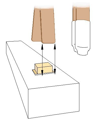
Figure 2
-
Lower the open clip over the LED and gently release the clip so it grasps the LED by the "sides". Very important: Grasp the LED slightly right-of-center as shown above so that the left side of the LED will be exposed past the left side of the clip as shown by the arrow positions above. This is to ensure the solder pad on the left side of the LED will be exposed for easy soldering when the Tool is turned over. See Figure 3 below.
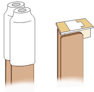
Figure 3
-
Turn the Holding Tool over and clamp its brass sheet base in your bench vise or whatever you will be using to secure it while it is on your workbench surface. If you use a bench vise, note that the bottom of the brass sheet is square and straight for easy alignment in a small vise. Note that the LED is offset slightly in the clip allowing the solder pad on the right to be totally exposed. This will make soldering to the pad much easier.
-
Since the LEDs are polarity sensitive devices, we use color-coded wiring to differentiate between the positive (+), and negative (-) electrical connections. In keeping with standard electrical conventions, we will connect the RED wire to the positive (+), or Anode solder pad of the LED (the electrically “hot” connection), and the GREEN wire to the negative (-), or Cathode solder pad (electrical “ground” connection). Remember that in the case of Red LEDs, the polarity mark points to the Anode (+) connection. For all other LEDs, the polarity mark points to the Cathode (-) connection. For all LEDs, the RED wire should be connected to the Anode solder pad.
-
Figure 3, above shows the back view of a typical Micro LED. Note the fat “T” shaped opening between the solder pads on each end of the LED. The base of the “T” points at the polarity mark. In this example, it points to the solder pad that is the Cathode, or negative (-) electrical connection. Another reminder is that (except for Red LEDs) the Cathode solder pad is shaped like a "C" (for cathode). Since the cathode solder pad is on the right, we will solder the GREEN wire first.
-
Figure 4 below, shows a tinned segment of green #38 magnet wire positioned over the cathode (-) solder pad of the LED. This is performed by gently holding open the padded clip while sliding the green wire into position over the solder pad, then releasing the padded clip to grip the wire. Center the wire over the pad and align the wire so that the insulated portion begins at the inside edge of the solder pad, as shown. This is easily done by opening and closing the padded clip with the right hand while adjusting the wire with the left hand. Position the wire so it lays flat against the pad. If necessary, a sharpened toothpick can be used to gently move the tinned portion front to back for best position.

Figure 4
-
In the next step, the wire will be soldered to the solder pad of the LED. Remember, these LEDs are very sensitive to thermal shock and excessive heat. Manufacture’s recommendations for soldering of these devices limits solder temperature to a maximum of 260ºC (500ºF), and a maximum contact time (soldering iron contact) of 2 seconds. In reality, since the wire has been pre-tinned and the solder pad is gold plated, actual contact time for acceptable solder flow should be much less that ½ second. A quick “touch” with a properly tinned iron having a tiny amount of low-temperature solder is all that will be required to complete the solder joint. As mentioned in the 2x3 LED wiring procedure, as an aid to the quick and even flow of the solder joint, we recommend placing a tiny (very tiny) amount of liquid flux at the point where the tinned wire and solder pad touch each other. Too much liquid flux will require cleanup.
-
Figure 5 below is an end view of two LEDs. The left view shows a good solder joint which has a low, smooth profile. The LED on the right has a solder joint with too much solder, which also contains peaks and a general irregular surface. Again a tiny bit of liquid flux will assist the quick and even flow of solder. An additional technique that will assist in getting a nice low-profile solder joint is shown in step 12 and Figure 6 below.
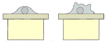
Figure 5
-
When positioning you iron tip over the part a technique that will help minimize the size of the solder "blob" that occurs at the solder pad & wire junction, is to contact the tinned portion of the wire with the molten solder just off the pad and allow it to "wick" onto the pad. The tinned wire will readily accept the molten solder and act like a wick drawing it up the wire. This method will give you much better control of the amount of solder that actually flows onto the solder pad. See Figure 6 below.
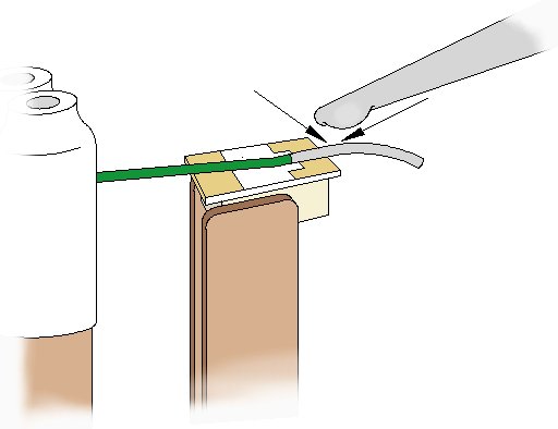
Figure 6
-
Figure 7, below shows the green wire soldered to the cathode (-) solder pad of the LED.
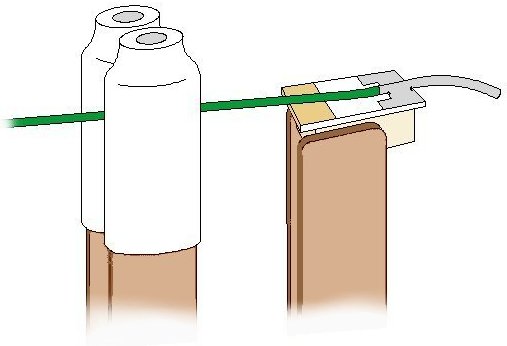
Figure 7
Click here to continue to next page...
© 2008 Ngineering